Assuming ideal op-smps, the circuit represents is
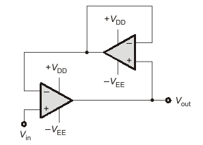
- Asumming amplifier
- Bdifference amplifier
- Clogarithmic amplifier
- Dbuffer
Solution & Step-by-step Explanation
The given circuit in the image is an operational amplifier (op-amp) configuration known as a buffer or voltage follower. Here’s how we determine that:
1. The op-amp is connected in a configuration where the output is directly connected to the inverting input. This is a common setup for a buffer circuit.
2. In a buffer circuit, the non-inverting input receives the input signal (V_{in}), while the output is connected to the inverting input, ensuring the output voltage (V_{out}) follows the input voltage.
3. This configuration provides a unity gain, meaning V_{out} = V_{in}. The main purpose of a buffer is to provide high input impedance, low output impedance, and to drive heavier loads without affecting the input signal.
Justification for the correct answer:
- Summing amplifier: This requires additional resistors at the input for summing multiple signals, which is not present here.
- Difference amplifier: This configuration requires specific resistor ratios and two inputs for taking the difference, which is not the case here.
- Logarithmic amplifier: This involves diodes or transistors within the feedback loop to achieve logarithmic behavior, not observed in this circuit.
- Buffer: As explained, the direct feedback connection and the single non-inverting input make it a buffer circuit.
Therefore, the circuit represents a buffer.
1. The op-amp is connected in a configuration where the output is directly connected to the inverting input. This is a common setup for a buffer circuit.
2. In a buffer circuit, the non-inverting input receives the input signal (V_{in}), while the output is connected to the inverting input, ensuring the output voltage (V_{out}) follows the input voltage.
3. This configuration provides a unity gain, meaning V_{out} = V_{in}. The main purpose of a buffer is to provide high input impedance, low output impedance, and to drive heavier loads without affecting the input signal.
Justification for the correct answer:
- Summing amplifier: This requires additional resistors at the input for summing multiple signals, which is not present here.
- Difference amplifier: This configuration requires specific resistor ratios and two inputs for taking the difference, which is not the case here.
- Logarithmic amplifier: This involves diodes or transistors within the feedback loop to achieve logarithmic behavior, not observed in this circuit.
- Buffer: As explained, the direct feedback connection and the single non-inverting input make it a buffer circuit.
Therefore, the circuit represents a buffer.