100% Free
GATE EC 2017 Question Paper (05-Feb-2017) (Shift 1)
Medium 65 Questions 180 min 100 marks
⚡ Live Test Mode Available
Take this as a timed mock test
180 min · 100 marks · Full test mode with leaderboard
Advertisement
Previous Year Questions
65medium5
Questions
0
Attempted
0
Correct
0
Wrong
0/5 attempted
Question No: 46Difficulty: mediumMarks: 2short_answer
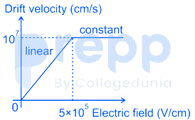
The dependence of drift velocity of electrons on electric field in a semiconductor is shown below. The semiconductor has a uniform electron concentration of n = 1 × 10¹⁶ cm and electronic charge q = 1.6 × 10 C. If a bias of 5 V is applied across a 1 μm region of this semiconductor, the resulting current density in this region, in kA/cm², is ________.
Question No: 47Difficulty: mediumMarks: 2short_answer
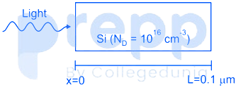
As shown, a uniformly doped Silicon (Si) bar of length L = 0.1 μm with a donor concentration N = 10¹⁶ cm is illuminated at x = 0 such that electron and hole pairs are generated at the rate of G = , where G = 10¹⁷ cm s.
Hole lifetime is 10 s, electronic charge q = 1.6 × 10 C, hole diffusion coefficient Dₚ = 100 cm²/s and low level injection condition prevails.
Assuming a linearly decaying steady sate excess hole concentration that goes to 0 at x = L, the magnitude of the diffusion current density at x = L/2, in A/cm², is ________.
Hole lifetime is 10 s, electronic charge q = 1.6 × 10 C, hole diffusion coefficient Dₚ = 100 cm²/s and low level injection condition prevails.
Assuming a linearly decaying steady sate excess hole concentration that goes to 0 at x = L, the magnitude of the diffusion current density at x = L/2, in A/cm², is ________.
Question No: 48Difficulty: mediumMarks: 2short_answer
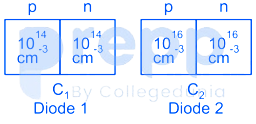
As shown, two Silicon (Si) abrupt p-n junction diodes are fabricated with uniform donor doping concentrations of N = 10¹⁴ cm and N = 10¹⁶ cm in the n-regions of the diodes, and uniform acceptor doping concentrations of N = 10¹⁴ cm and N = 10¹⁶ cm in the p-regions of the diodes, respectively. Assuming that the reverse bias voltage is ≫ built-in potentials of the diodes, the ratio C₂/C₁ of their reverse bias capacitances for the same applied reverse bias, is ________.
Question No: 49Difficulty: mediumMarks: 2short_answer
In the figure shown, the npn transistor acts as a switch
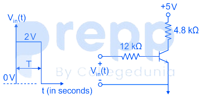
For the input Vᵢₙ(t) as shown in the figure, the transistor switches between the cut-off and saturation regions of operation, when T is large. Assume collector-to-emitter voltage at saturation V = 0.2V and base-to-emitter voltage V = 0.7V. The minimum value of the common-base current gain (α) of the transistor for the switching should be ________.
For the input Vᵢₙ(t) as shown in the figure, the transistor switches between the cut-off and saturation regions of operation, when T is large. Assume collector-to-emitter voltage at saturation V = 0.2V and base-to-emitter voltage V = 0.7V. The minimum value of the common-base current gain (α) of the transistor for the switching should be ________.
Question No: 50Difficulty: mediumMarks: 2short_answer
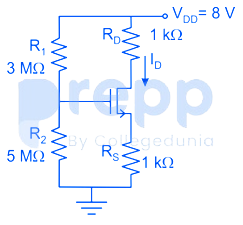
For the circuit shown, assume that the NMOS transistor is in saturation. Its threshold voltage Vₜₙ = 1 V and its transconductance parameter Neglect channel length modulation and body bias effects. Under these conditions, the drain current I in mA is ________.
✓ Showing questions 46–50 of 65 — use the page buttons below to practice the rest
You May Also Like
📊 Track Your Progress
Know exactly where you stand
Save scores, track weak topics, compare with toppers — all free.
Advertisement