100% Free
GATE EC 2017 Question Paper (05-Feb-2017) (Shift 2)
Medium 65 Questions 180 min 100 marks
⚡ Live Test Mode Available
Take this as a timed mock test
180 min · 100 marks · Full test mode with leaderboard
Advertisement
Previous Year Questions
65medium5
Questions
0
Attempted
0
Correct
0
Wrong
0/5 attempted
Question No: 46Difficulty: mediumMarks: 2short_answer
A MOS capacitor is fabricated on p-type Si (Silicon) where the metal work function is 4.1 eV and electron affinity of Si is 4.0 eV. E - E = 0.9 eV, where E and E are the conduction band minimum and the Fermi energy levels of Si, respectively. Oxide ϵᵣ = 3.9, ϵₒ = 8.85 × 10⁻¹⁴ F/cm, oxide thickness tₒₓ = 0.1 μm and electronic charge q = 1.6 × 10⁻¹⁹ C. If the measured flat band voltage of this capacitor is -1 V, then the magnitude of the fixed charge at the oxide-semiconductor interface, in nC/cm², is ________.
Question No: 47Difficulty: mediumMarks: 2short_answer
For a particular intensity of incident light on a silicon p-n junction solar cell, the photocurrent density (J) is 2.5 mA/cm² and the open-circuit voltage (V) is 0.451 V. Consider thermal voltage (V) to be 25 mV. If the intensity of the incident light is increased by 20 times, assuming that the temperature remains unchanged, V (in volts) will be ___________.
(Take the ideality factor, η = 2 for Silicon)
(Take the ideality factor, η = 2 for Silicon)
Question No: 48Difficulty: mediumMarks: 2mcq
Two n-channel MOSFETs, T1 and T2, are identical in all respects except that the width of T2 is double that of T1. Both the transistors are biased in the saturation region of operation, but the gate overdrive voltage (V - V) of T2 is double that of T1, where V and V are the gate-to-source voltage and threshold voltage of the transistors, respectively. If the drain current and transconductance of T1 are I and g respectively, the corresponding values of these two parameters for T2 are
Question No: 49Difficulty: mediumMarks: 2mcq
An abrupt p-n junction (located at x = 0) is uniformly doped on both p and n sides. The width of the depletion region is W and the electric field variation in the x-direction is E(x). Which of the following figures represents the electric field profile near the p-n junction?
Question No: 50Difficulty: mediumMarks: 2mcq
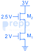
Assuming that transistors M₁ and M₂ are identical and have a threshold voltage of 1 V, the state of transistors M₁ and M₂ are respectively
✓ Showing questions 46–50 of 65 — use the page buttons below to practice the rest
You May Also Like
📊 Track Your Progress
Know exactly where you stand
Save scores, track weak topics, compare with toppers — all free.
Advertisement