100% Free
GATE EC 2017 Question Paper (05-Feb-2017) (Shift 2)
Medium 65 Questions 180 min 100 marks
⚡ Live Test Mode Available
Take this as a timed mock test
180 min · 100 marks · Full test mode with leaderboard
Advertisement
Previous Year Questions
65medium5
Questions
0
Attempted
0
Correct
0
Wrong
0/5 attempted
Question No: 51Difficulty: mediumMarks: 2short_answer
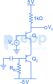
In the circuit shown, transistors Q₁ and Q₂ are biased at a collector current of 2.6 mA. Assuming that transistor current gains are sufficiently large to assume collector current equal to emitter current and thermal voltage of 26 mV, the magnitude of voltage gain Vₒ/Vₛ in the mid-band frequency range is ___________ (up to second decimal place).
Question No: 52Difficulty: mediumMarks: 2short_answer
In the voltage reference circuit shown in the figure, the op-amp is ideal and the transistors Q₁, Q₂… Q₃₂ are identical in all respects and have infinitely large values of common-emitter current gain (β). The collector current (I) of the transistors is related to their base-emitter voltage (V) by the relation I = I exp (V /V), where I is the saturation current. Assume that the voltage Vₚ shown in the figure is 0.7 V and the thermal voltage V = 26 mV.
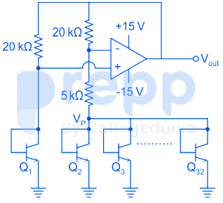
The output voltage Vₒᵤₜ (in volts) is _________
The output voltage Vₒᵤₜ (in volts) is _________
Question No: 53Difficulty: mediumMarks: 2short_answer
The state diagram of a finite state machine (FSM) designed to detect an overlapping sequence of three bits is shown in the figure. The FSM has an input ‘In’ and an output ‘Out’. The initial state of the FSM is S₀.
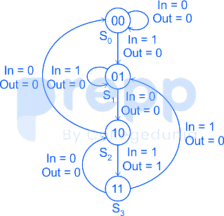
If the input sequence is 10101101001101, starting with the left-most bit, then the number of times ‘Out’ will be 1 is _________
If the input sequence is 10101101001101, starting with the left-most bit, then the number of times ‘Out’ will be 1 is _________
Question No: 54Difficulty: mediumMarks: 2short_answer
Figure I shows a 4-bit ripple carry adder realized using full adders and Figure II shows the circuit of a full-adder (FA). The propagation delay of the XOR, AND and OR gates in Figure II are 20 ns, 15 ns and 10 ns, respectively. Assume all the inputs to the 4-bit adder are initially reset to 0.
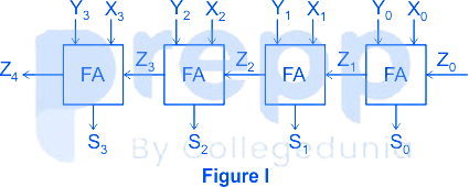
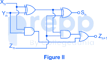
At t = 0, the inputs to the 4-bit adder are changed to X₃X₂X₁X₀ = 1100, Y₃Y₂Y₁Y₀ = 0100 and Z₀ = 1. The output of the ripple carry adder will be stable at t (in ns) = ____________
At t = 0, the inputs to the 4-bit adder are changed to X₃X₂X₁X₀ = 1100, Y₃Y₂Y₁Y₀ = 0100 and Z₀ = 1. The output of the ripple carry adder will be stable at t (in ns) = ____________
Question No: 55Difficulty: mediumMarks: 2mcq
A programmable logic array (PLA) is shown in the figure.
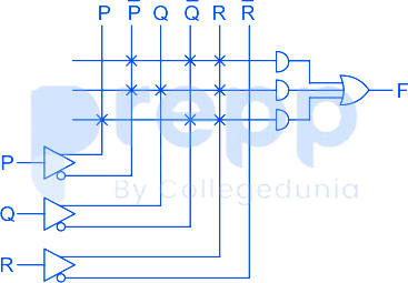
The Boolean function F implemented is
The Boolean function F implemented is
✓ Showing questions 51–55 of 65 — use the page buttons below to practice the rest
You May Also Like
📊 Track Your Progress
Know exactly where you stand
Save scores, track weak topics, compare with toppers — all free.
Advertisement