Physics
Semiconductors Questions
39 Semiconductors questions from Physics with detailed answers and explanations. Free previous year questions and MCQs.
📚
39
Questions
🟢
11
Easy
🟡
26
Medium
🔴
2
Hard
Semiconductors — Physics(1–39 of 39)
Filter:
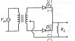
A full wave rectifier circuit with diodes () and () is shown in the figure. If input supply voltage , then at :
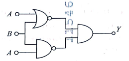
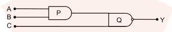
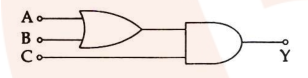
The output () of the given logic implementation is similar to the output of an/a _________ gate.
A transistor is operated in common emitter configuration at such that a change in the base current from to produces a change in the collector current from to . The current gain is:
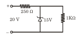
A Zener diode with is used in a regulator with and . Current through diode is:
What is the output in the following circuit, when all the three inputs are first 0 and then 1?
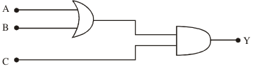
To get an output in the given circuit (AND gate with inputs and then OR gate with ), which of the following input will be correct:
Silicon transistor input resistance is . Base current changes by resulting in collector current change of . For a load resistance of in common emitter, voltage gain is:
and both have same lattice structure, having bonding electrons in each. However, is insulator whereas is intrinsic semiconductor. This is because:
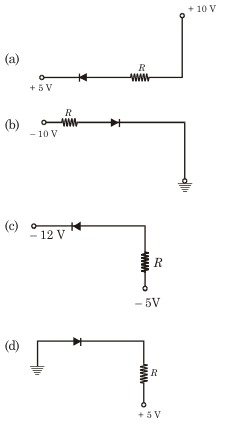
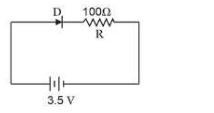
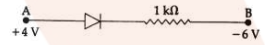
In the given figure, a diode is connected to an external resistance and an e.m.f. of . If the barrier potential developed across the diode is , the current in the circuit will be:
To get output 1 for the following circuit, the correct choice for the input is:
Consider the junction diode as ideal. The value of current flowing through is:
A transistor is connected in common emitter configuration in a given amplifier. A load resistance of is connected in the collector circuit and the voltage drop across it is . If the current amplification factor is and the input resistance of the circuit is , the voltage gain and the power gain of the amplifier will respectively be:
For CE transistor amplifier, the audio signal voltage across the collector resistance of is . If the current amplification factor of the transistor is and the base resistance is , then the input signal voltage is:
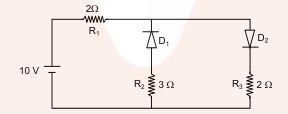
The given circuit has two ideal diodes connected as shown in the figure below. The current flowing through the resistance will be:
In the following circuit, the output for all possible inputs and is expressed by the truth table:ShutterstockExplore
Consider an - - transistor amplifier in common-emitter configuration. The current gain of the transistor is . If the collector current changes by , what will be the change in emitter current?
In a semiconducting material the mobilities of electrons and holes are and respectively. Which of the following is true?
Assertion: The logic gate NOT can be built using diode.Reason: The output voltage and the input voltage of the diode have phase difference.
Assertion: The number of electrons in a -type silicon semiconductor is less than the number of electrons in a pure silicon semiconductor at room temperature.Reason: It is due to law of mass action.
Assertion: In a common emitter transistor amplifier the input current is much less than the output current.Reason: The common emitter transistor amplifier has very high input impedance.
A transistor-oscillator using a resonant circuit with an inductance (of negligible resistance) and a capacitance has a frequency . If is doubled and is changed to , the frequency will be:
A transistor is operated in common emitter configuration at constant collector voltage such that a change in the base current from to produces a change in the collector current from to . The current gain () is:
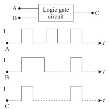
The following figure shows a logic gate circuit with two inputs A and B and the output C. The voltage waveforms of A, B, and C as shown below:(Assuming waveforms where C is high only when both A and B are high, matching a standard AND gate profile)The logic circuit gate is :
In the energy band diagram of a material shown below, the open circles and filled circles denote holes and electrons respectively. The material is a/an:
A common emitter amplifier has a voltage gain of , an input impedance of and an output impedance of . The power gain of the amplifier is:
The voltage gain of an amplifier with negative feedback is . The voltage gain without feedback will be:
A p-n photodiode is made of a material with a band gap of . The minimum frequency of the radiation that can be absorbed by the material is nearly:
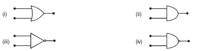
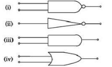
The symbolic representations of four logic gates are given. The symbols for OR, NOT and NAND gates are respectively:
A p-n photodiode is fabricated from a semiconductor with a band gap of . It can detect a signal of wavelength:
Physics Semiconductors — FAQ
How many Semiconductors questions come in Physics?▼
Our database has 39 Semiconductors questions from Physics.
What difficulty are Physics Semiconductors questions?▼
The 39 Physics Semiconductors questions include 11 easy, 26 medium and 2 hard level questions.
Where can I find more Semiconductors questions for other exams?▼
Visit /tag/semiconductors to see all Semiconductors questions across all exams including NEET 2017, AIEEE 2003, NEET 2019.