HomeTestsSearchRankProfile

Semiconductors Questions

Practice 57 Semiconductors questions with detailed answers and explanations. Free MCQs, PYQs, and mock test questions for NEET, JEE, GATE, SSC and more.

📚
57
Total Questions
🟢
19
Easy
🟡
36
Medium
🔴
2
Hard
Practice by Exam:Physics(56)Chemistry(1)

About Semiconductors — practice questions, PYQs & concepts

Semiconductors is a frequently-tested topic on Physics, Chemistry. ExamTest.live currently lists 57 Semiconductors questions spanning previous-year papers from 2026 to 2026, each with worked solutions and a step-by-step explanation. Use the filters on this page to focus on a specific exam, difficulty level or year — every answer key is free, no sign-up required.

Semiconductors weight in competitive exams

Across our Semiconductors question bank, the largest sources are Physics (56) and Chemistry (1). Click any exam chip above to drill down to that exam-specific question set.

How to use this page

  • Start easy: 19 easy Semiconductors questions are available — build fluency before moving up.
  • Target weak years: Use the year filter to focus on the most recent 2026 paper or older PYQs you have not attempted.
  • Time yourself: Every question shows the average solve time so you can benchmark your speed against other students.
  • Read every explanation: Even on questions you got right — the explanation often surfaces a faster approach you can reuse.

All Semiconductors Questions(157 of 57)

Filter:
Q1easymcqPhysicsAIEEE 20042026
50% accuracy
A piece of copper and another of germanium are cooled from room temperature to . The resistance of:
Q2mediummcqPhysicsAIEEE 20072026
0% accuracy
Carbon, silicon and germanium have four valence electrons each. At room temperature which one of the following statements is most appropriate?
Q3mediummcqPhysicsAIEEE 20072026
0% accuracy
If in a p-n junction diode, a square input signal of is applied as shown
image
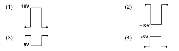
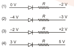
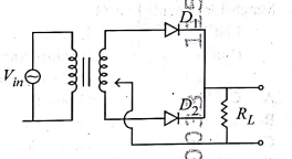
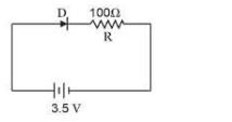
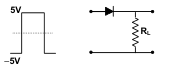
, then the output signal across a load resistance (connected in series with the diode) will be:
image
Q4easymcqPhysicsNEET 20192026
0% accuracy
For a p-type semiconductor, which of the following statements is true?
Q5mediummcqPhysicsNEET 20192026
0% accuracy
The correct Boolean operation represented by the circuit diagram drawn is:
image
Q6easymcqPhysicsAIEEE2026
In a common base amplifier, the phase difference between the input signal voltage and output voltage is:
Q7mediummcqPhysicsNEET 20172026
In a common emitter transistor amplifier the audio signal voltage across the collector is . The resistance of collector is . If current gain is and the base resistance is , the voltage and power gain of the amplifier is:
Q8easymcqPhysicsNEET 20172026
Which one of the following represents forward bias diode?
image
Q9easymcqPhysicsNEET 20172026
The given electrical network is equivalent to:
image
Q10easymcqPhysicsNEET 2020 E12026
The solids which have the negative temperature coefficient of resistance are:
Q11mediummcqPhysicsNEET (UG) 20242026
Consider the following statements A and B and identify the correct answer:A. For a solar-cell, the I-V characteristics lies in the IV quadrant of the given graph.B. In a reverse biased pn junction diode, the current measured in (), is due to majority charge carriers.
image
Q12mediummcqPhysicsAIEEE2026
The electrical conductivity of a semiconductor increases when electromagnetic radiation of wavelength shorter than is incident on it. The band gap in () for the semiconductor is:
Q13mediummcqPhysicsAIEEE 20032026
The difference in the variation of resistance with temperature in a metal and a semiconductor arises essentially due to the difference in the:
Q14mediummcqPhysicsAIEEE 20032026
In the middle of the depletion layer of a reverse-biased p-n junction, the:
Q15easymcqPhysicsAIEEE 20032026
A strip of copper and another of germanium are cooled from room temperature to . The resistance of:
Q16mediummcqPhysicsJEE Main2026
The characteristic of an LED is:
image
Q17mediummcqPhysicsIndian Competitive Exams2026
Which element is used for making solar cells?
Q18mediummcqPhysicsPhysics
0% accuracy
A full wave rectifier circuit with diodes () and () is shown in the figure. If input supply voltage , then at :

image
Q19mediummcqPhysicsPhysics
6% accuracy
The output () of the given logic implementation is similar to the output of an/a _________ gate.

image
Q20mediummcqPhysicsPhysics
0% accuracy
A transistor is operated in common emitter configuration at such that a change in the base current from to produces a change in the collector current from to . The current gain is:
Q21mediummcqPhysicsPhysics
0% accuracy
If a small amount of antimony is added to germanium crystal:
Q22mediummcqPhysicsPhysics
0% accuracy
In forward biasing of the - junction:
Q23mediummcqPhysicsPhysics
0% accuracy
Symbolic representation of four logic gates are shown as:(i) OR gate AND gate NOT gate [NAND gate]Pick out which ones are for AND, NAND and NOT gates, respectively:
image
Q24easymcqChemistryChemistry
With which one of the following elements silicon should be doped so as to give p-type of semiconductor?
Q25hardmcqPhysicsPhysics
For CE transistor amplifier, the audio signal voltage across the collector resistance of is . If the current amplification factor of the transistor is and the base resistance is , then the input signal voltage is:
Q26hardmcqPhysicsPhysics
A p-n photodiode is made of a material with a band gap of . The minimum frequency of the radiation that can be absorbed by the material is nearly:
Q27mediummcqPhysicsPhysics
The circuit shown is equivalent to:
Q28mediummcqPhysicsPhysics
The voltage gain of an amplifier with negative feedback is . The voltage gain without feedback will be:
Q29mediummcqPhysicsPhysics
A common emitter amplifier has a voltage gain of , an input impedance of and an output impedance of . The power gain of the amplifier is:
Q30easymcqPhysicsPhysics
In the energy band diagram of a material shown below, the open circles and filled circles denote holes and electrons respectively. The material is a/an:
Q31mediummcqPhysicsPhysics
In the following circuit, the output for all possible inputs and is expressed by the truth table:ShutterstockExplore
Q32mediummcqPhysicsPhysics
The following figure shows a logic gate circuit with two inputs A and B and the output C. The voltage waveforms of A, B, and C as shown below:(Assuming waveforms where C is high only when both A and B are high, matching a standard AND gate profile)The logic circuit gate is :
image
Q33easymcqPhysicsPhysics
Which of the following is an example of forward biasing?
Q34mediummcqPhysicsPhysics
A transistor is operated in common emitter configuration at constant collector voltage such that a change in the base current from to produces a change in the collector current from to . The current gain () is:
Q35mediummcqPhysicsPhysics
A transistor-oscillator using a resonant circuit with an inductance (of negligible resistance) and a capacitance has a frequency . If is doubled and is changed to , the frequency will be:
Q36mediummcqPhysicsPhysics
Assertion: In a common emitter transistor amplifier the input current is much less than the output current.Reason: The common emitter transistor amplifier has very high input impedance.
Q37mediummcqPhysicsPhysics
Assertion: The number of electrons in a -type silicon semiconductor is less than the number of electrons in a pure silicon semiconductor at room temperature.Reason: It is due to law of mass action.
Q38easymcqPhysicsPhysics
Assertion: The logic gate NOT can be built using diode.Reason: The output voltage and the input voltage of the diode have phase difference.
Q39easymcqPhysicsPhysics
In a semiconducting material the mobilities of electrons and holes are and respectively. Which of the following is true?
Q40mediummcqPhysicsPhysics
Consider an - - transistor amplifier in common-emitter configuration. The current gain of the transistor is . If the collector current changes by , what will be the change in emitter current?
Q41easymcqPhysicsPhysics
and both have same lattice structure, having bonding electrons in each. However, is insulator whereas is intrinsic semiconductor. This is because:
Q42mediummcqPhysicsPhysics
A p-n photodiode is fabricated from a semiconductor with a band gap of . It can detect a signal of wavelength:
Q43easymcqPhysicsPhysics
A transistor is operated in common-emitter configuration at such that a change in the base current from to produces a change in the collector current from to . The current gain is:
Q44easymcqPhysicsPhysics
Which of the following statements is False?
Q45mediummcqPhysicsPhysics
A Zener diode with is used in a regulator with and . Current through diode is:
image
Q46mediummcqPhysicsPhysics
In which of the following figures are the diodes forward biased?
image
Q47mediummcqPhysicsPhysics
Pure at has . Doping by Indium increases to . The doped semiconductor is:
Q48easymcqPhysicsPhysics
To get an output in the given circuit (AND gate with inputs and then OR gate with ), which of the following input will be correct:
image
Q49mediummcqPhysicsPhysics
Silicon transistor input resistance is . Base current changes by resulting in collector current change of . For a load resistance of in common emitter, voltage gain is:
Q50mediummcqPhysicsPhysics
What is the output in the following circuit, when all the three inputs are first 0 and then 1?
image
Q51easymcqPhysicsPhysics
In a n-type semiconductor, which of the following is true?
Q52easymcqPhysicsPhysics
In the given figure, a diode is connected to an external resistance and an e.m.f. of . If the barrier potential developed across the diode is , the current in the circuit will be:
image
Q53mediummcqPhysicsPhysics
To get output 1 for the following circuit, the correct choice for the input is:
image
Q54easymcqPhysicsPhysics
Consider the junction diode as ideal. The value of current flowing through is:
image
Q55mediummcqPhysicsPhysics
A transistor is connected in common emitter configuration in a given amplifier. A load resistance of is connected in the collector circuit and the voltage drop across it is . If the current amplification factor is and the input resistance of the circuit is , the voltage gain and the power gain of the amplifier will respectively be:
Q56mediummcqPhysicsPhysics
The symbolic representations of four logic gates are given. The symbols for OR, NOT and NAND gates are respectively:
image
Q57mediummcqPhysicsPhysics
The given circuit has two ideal diodes connected as shown in the figure below. The current flowing through the resistance will be:
image

Frequently Asked Questions

How many Semiconductors questions are on ExamTest.live?
We have 57 Semiconductors questions spread across 1 pages, covering easy, medium, and hard difficulty levels with detailed explanations.
Are Semiconductors MCQs free?
Yes. All Semiconductors questions, answers, and explanations on ExamTest.live are completely free. No account or subscription required.
Which exams include Semiconductors questions?
Semiconductors questions are commonly asked in Physics, Chemistry. You can filter by exam using the links above.
How do I practice Semiconductors questions effectively?
Start with easy questions to build confidence, then tackle medium and hard ones. Use the filter buttons to sort by difficulty. Reveal the answer only after attempting each question, and read the explanation thoroughly.