100% Free
PYQs Based Test - 13 : Electronic Devices
Medium 20 Questions 180 min 32 marks
⚡ Live Test Mode Available
Take this as a timed mock test
180 min · 32 marks · Full test mode with leaderboard
Advertisement
Previous Year Questions
20medium5
Questions
0
Attempted
0
Correct
0
Wrong
0/5 attempted
Question No: 1Difficulty: mediumMarks: 1mcq
The doping concentrations on the p-side and n-side of a silicon diode are 1 × 10¹⁶ cm⁻³ and 1 × 10¹⁷ cm⁻³, respectively. The forward bias of 0.3 V is applied to the diode. At T = 300 K, the intrinsic carrier concentration of silicon nᵢ = 1.5 × 10¹⁰ and . The electron concentration at the edge of the depletion region p-side is
Question No: 2Difficulty: mediumMarks: 2short_answer
The slope of the I vs. V curve of an n-channel MOSFET in linear regime is 10⁻³ Ω⁻¹ at V = 0.1 V. For the same device, neglecting channel length modulation, the slope of the vs. V curve (in ) under saturation regime is approximately ______
Question No: 3Difficulty: mediumMarks: 1mcq
The quantum efficiency (η) and responsivity (R) at a wavelength λ (in μm) in a p-i-n photodetector are related by
Question No: 4Difficulty: mediumMarks: 2short_answer
A silicon P-N junction is shown in the figure. The doping in the P region is 5 × 10¹⁶ cm⁻³ and doping in the N region is 10 × 10¹⁶ cm⁻³. The parameters given are
Built-in voltage (Φ) = 0.8 V
Electron charge (q) = 1.6 × 10⁻¹⁹ C
Vacuum permittivity (ε₀) = 8.85 × 10⁻¹² F / m
Relative permittivity of silicon (ε) = 12
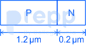
The magnitude of reverse bias voltage that would completely deplete one of the two regions (P or N) prior to the other (rounded off to one decimal place) is _______ V.
Built-in voltage (Φ) = 0.8 V
Electron charge (q) = 1.6 × 10⁻¹⁹ C
Vacuum permittivity (ε₀) = 8.85 × 10⁻¹² F / m
Relative permittivity of silicon (ε) = 12
The magnitude of reverse bias voltage that would completely deplete one of the two regions (P or N) prior to the other (rounded off to one decimal place) is _______ V.
Question No: 5Difficulty: mediumMarks: 2short_answer
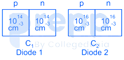
As shown, two Silicon (Si) abrupt p-n junction diodes are fabricated with uniform donor doping concentrations of N = 10¹⁴ cm and N = 10¹⁶ cm in the n-regions of the diodes, and uniform acceptor doping concentrations of N = 10¹⁴ cm and N = 10¹⁶ cm in the p-regions of the diodes, respectively. Assuming that the reverse bias voltage is ≫ built-in potentials of the diodes, the ratio C₂/C₁ of their reverse bias capacitances for the same applied reverse bias, is ________.
✓ Showing questions 1–5 of 20 — use the page buttons below to practice the rest
You May Also Like
📊 Track Your Progress
Know exactly where you stand
Save scores, track weak topics, compare with toppers — all free.
Advertisement